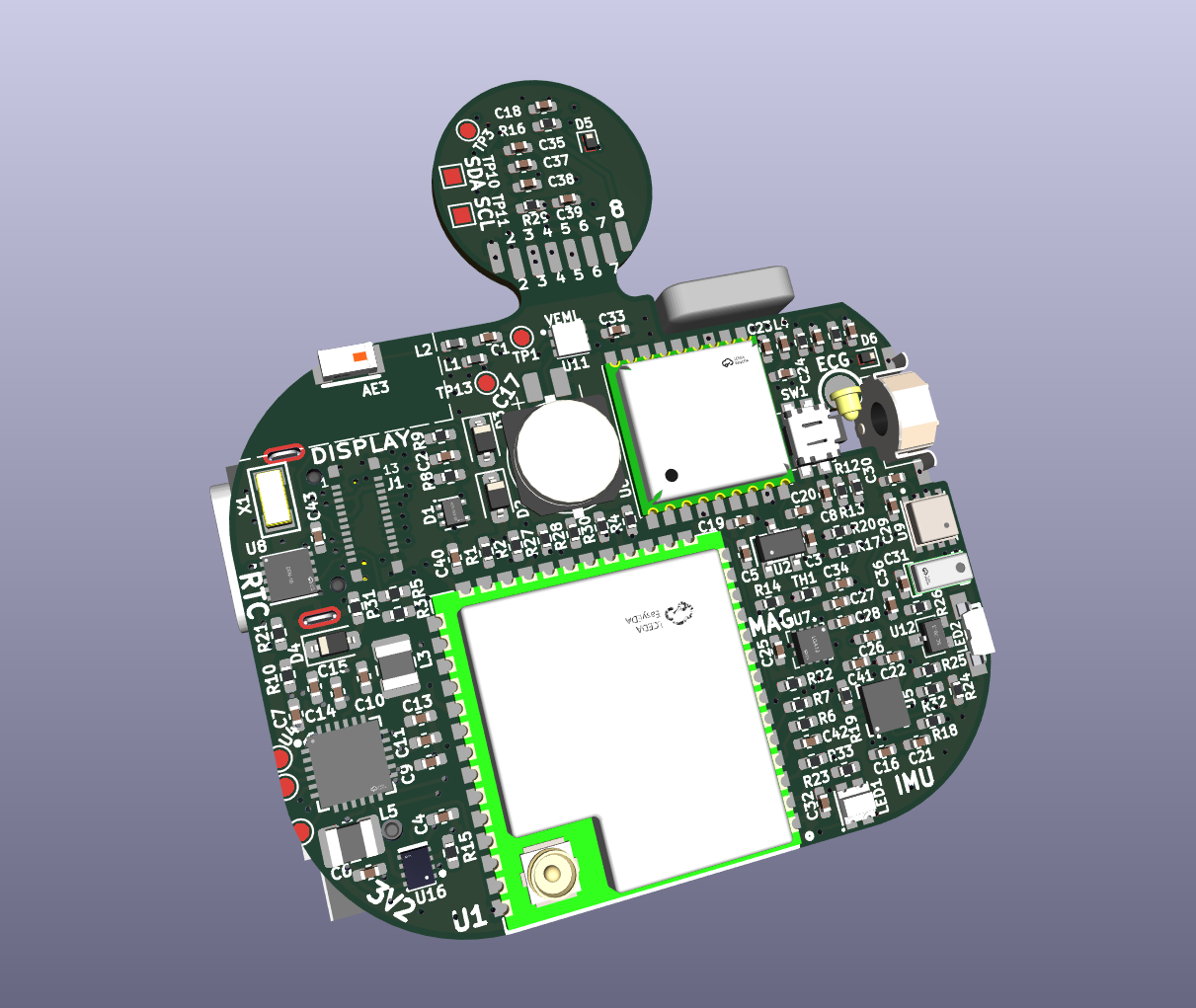
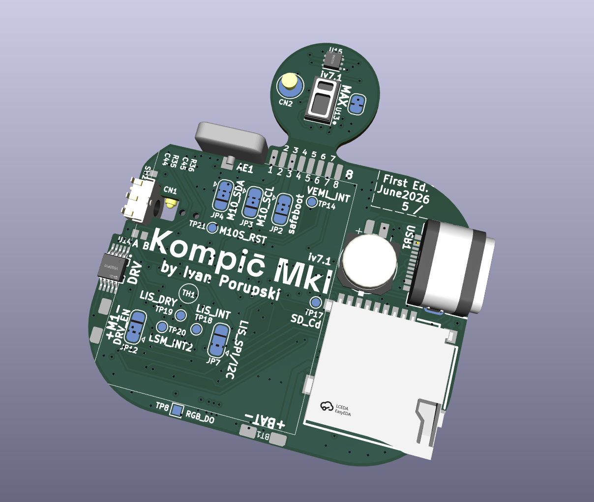
Fabrication and Assembly
First Run in Preparation
A finished Kompic̄ comes together in four stages — two at the manufacturer, two on the bench:
- Fabrication — the bare 4-layer PCB is produced from the Gerbers.
- Machine assembly — the economy PCBA service places the small passives.
- Reflow — the remaining top-side parts are hand-placed and hot-plate reflowed in a single pass.
- Manual soldering & wiring — the underside parts, the USB-C jack, and the wired sub-assemblies are finished by hand.
The split is driven by cost and process limits:
- 4-layer, 1 mm. Four layers to route the density on a 44.5 × 50.62 mm outline; 1 mm to keep the case stack thin.
- Machine assembly is top-side and passives-only. One stencil, one pass, lowest cost.
- The costly parts and the hand-finished parts stay off the machine. Partly to keep a small prototype run affordable, partly because some parts (the underside components, the wired sub-assemblies) simply can't be machine-placed.
Manufacturer Recommendation
The production files in the repository were generated by JLCPCB's tooling, and the author used JLCPCB and their economy PCBA out of familiarity. This is not an endorsement — any capable fabricator and assembler will do; choose one for your needs and regenerate the files for their workflow if required.
1 · Fabricating the Bare Board
The KiCad project and production files live in the repository under
hardware/Kompic_Mk1.
Upload the production set to the manufacturer's quote tool — three files do the work:
- the Gerber .zip — copper, mask, and silkscreen artwork,
- the BOM — the bill of materials for the assembled parts, and
- the placement file — the position and rotation of each assembled part.
Most fabrication settings stay at their defaults. Two were changed:
Non-default settings
Thickness → 1 mm (from the usual 1.6 mm). The watch has a tight thickness budget; a thinner board buys back room in the case stack.
Surface finish → lead-free HASL (from leaded). The same flat, solderable finish without the lead.
The board outline is 44.5 × 50.62 mm. Main and daughter board are panelized as a single 4-layer design on this one outline and routed apart after fabrication. Five sets were ordered for the first run.
Full fabrication settings used for this order
| Base material | FR-4 (TG135) |
| Layers | 4 |
| Dimension | 44.5 mm × 50.62 mm |
| PCB thickness | 1 mm (changed) |
| Surface finish | Lead-free HASL (changed) |
| Outer copper weight | 1 oz |
| Inner copper weight | 0.5 oz |
| PCB color | Green |
| Silkscreen | White |
| Via covering | Plugged |
| Min. via hole / diameter | 0.3 mm / 0.4–0.45 mm |
| Delivery format | Single PCB |
| PCB quantity | 5 |
| Electrical test | Flying-probe, full test |
| Board outline tolerance | ±0.2 mm |
| Appearance quality | IPC Class 2 |
2 · Machine Assembly (Economy PCBA)
The economy PCBA service machine-places the passives on the top side. The order ran on stock defaults — nothing was changed from what the economy tier ships with (top-side only, high-temp paste, nitrogen reflow, 5 boards).
Full economy PCBA settings used for this order
| PCBA type | Economic |
| Assembly side | Top side |
| PCBA quantity | 5 |
| Tooling holes | Added by manufacturer |
| Confirm parts placement | No |
| Bake components | No |
| Photo confirmation | No |
| Board cleaning | No |
| Conformal coating | No |
| Special stencil | No |
| Solder paste | High temp. |
| Nitrogen reflow | Yes (economy default) |
| Flying-probe test | No |
| Function test | No |
| Depanel before delivery | No |
| Panel format | 1 × 1 |
| Packaging | Antistatic bubble film |
| File provided as | Complete file (own files) |
| Build time | 3–4 days |
These are the 14 line items actually placed by the machine — straight from the assembler's selected-parts export, with LCSC part numbers and library tier:
| Value / Part | Designators | LCSC | Tier |
|---|---|---|---|
| Capacitors (0402) | |||
| 10 µF | C2, C3, C5, C6, C9, C11, C13, C14 | C15525 | Basic |
| 4.7 µF | C4, C22, C27, C35 | C23733 | Basic |
| 1 µF | C7, C15, C34, C36, C37 | C52923 | Basic |
| 100 nF (decoupling) | C8, C10, C16, C19, C20, C25, C26, C28–C33, C38–C45 | C1525 | Basic |
| 100 pF | C18, C21 | C1546 | Basic |
| 1.0 pF (BLE match) | C1 | C1550 | Extended |
| Resistors (0402) | |||
| 10 kΩ | R1, R2, R4, R10, R13, R14, R17, R20, R24, R27, R28, R30, R31, R33, R35, R36 | C25744 | Basic |
| 5.1 kΩ (I²C / pull-ups) | R3, R5–R9, R12, R19, R21, R22, R29 | C25905 | Basic |
| 470 Ω (Qvar RC) | R16, R18 | C25117 | Basic |
| 100 kΩ (TPS62840 VSET → 3.2 V) | R15 | C25741 | Basic |
| 47 Ω | R23, R25, R26, R32 | C25118 | Extended |
| Diode | |||
| 1N4148WS (SOD-323) | D2, D3, D4 | C2128 | Basic |
| Active / sensing | |||
| 10 kΩ NTC (charger temp sense) | TH1 | C77131 | Extended |
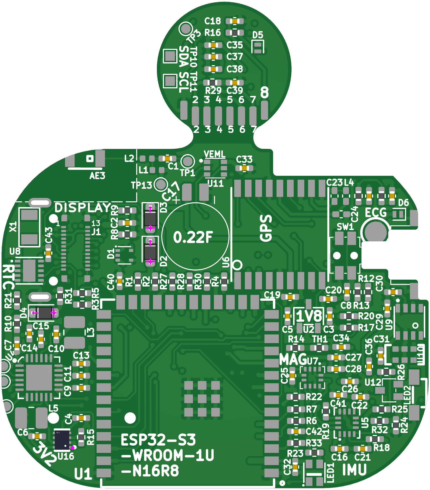
| TPS62840DLCR buck (→ 3.2 V rail) | U16 | C2071859 | Extended |
Basic vs Extended — why most rows say "Basic"
Basic parts live in the assembler's standing feeders and carry no setup fee. Extended parts are loaded from the wider catalogue and each one adds a per-part setup fee (roughly $3), which piles up fast across a BOM.
So the design was steered onto Basic parts wherever one would do. Only four Extended parts survive, because nothing Basic fit them: the 1.0 pF RF match cap, the 47 Ω resistor, the NTC thermistor, and the TPS62840 buck.
Verify orientation and polarity of every part in the assembler's viewer before approving the order. The design-for-manufacturability pass catches a lot, but treat it as a safety net, not a substitute for the check.
Why an IC (the buck) is in the machine set
The TPS62840 buck (U16) is the one IC here rather than on the reflow tray — it was meant to be hand-placed but slipped into the machine BOM. Rather than re-spin the order it was left in PCBA; the only correction needed was its placement orientation in the viewer before approval. Expect calls like this: a part goes out of stock, lands on the wrong list, or turns out cheaper to assemble than to hand-place, and you adjust the split accordingly.
3 · Reflow (Hand-Placed, Single Pass)
The remaining top-side parts — the module, sensors, the inductors and TVS kept off the machine set, connectors, and discretes — are placed by hand and hot-plate reflowed.
One pass, no second go
Everything reflowable goes down in a single pass. There's no second reflow for any part, the GPS module included — once the board is hand-finished (the USB-C jack especially) it can't safely go back on the hot plate, so all reflow happens here, first.
Why hand-place these
Hand-sourcing and reflowing the expensive parts keeps a prototype run affordable: roughly 50€ in parts for one or two watches, against 200€+ to fully assemble all five boards. Prove the design on a couple of units, then commit to a populated run.
| Designator | Part | Notes |
|---|---|---|
| Main-board ICs | ||
| U1 | ESP32-S3-WROOM-1U-N16R8 | MSL3 — bake if open >1 week |
| U2 | XC6206P182MR | 1.8 V LDO |
| U4 | BQ25619RTWR | charger + boost |
| U5 | LSM6DSV16XTR | IMU + Qvar ECG |
| U6 | MAX-M10S | GPS — MSL3 |
| U7 | LIS3MDLTR | magnetometer |
| U8 | PCF85063ATL | RTC |
| U9 | BME688 | environmental |
| U10 | MSM261DGT003 | PDM MEMS mic |
| U11 | VEML6030 | ambient light |
| U12 | BSS138W | level-shift MOSFET |
| Daughter board | ||
| U13 | MAX30101EFD+T | optical HR / SpO&sub2; |
| U15 | TMP117AIDRVR | skin temperature |
| Inductors (kept off the machine set) | ||
| L1 | 2.7 nH | BLE match |
| L2 | 3.9 nH | BLE match |
| L4 | 27 nH | GPS bias-T |
| L3, L5 | 2.2 µH (1008) | BQ25619 & TPS62840 switchers |
| Connectors, RF & discrete | ||
| J1 | OK-F024-04 | 24-pin display connector |
| D1 | TPD2E001DRLR | USB data-line TVS |
| D5, D6 | ESDALCL5-1BM2 | 5 V rail TVS |
| AE3 | 2450AT18A100E | BLE chip antenna |
| LED1 | WS2812B-2020 | addressable RGB |
| LED2 | TJ-S4008SW4 | flashlight LED |
| X1 | FC31M2 32.768 kHz | RTC crystal |
| C17 | 0.22 F supercap | GPS backup |
The hot-plate profile and the MSL3 bake notes for the module and GPS are in the Manual Assembly guide →
4 · Manual Soldering & Wiring
What's left is finished by hand, with a soldering iron or a hot-air station — the underside parts (which never face the hot plate), the USB-C jack, and the wired sub-assemblies.
| Designator | Part | Notes |
|---|---|---|
| Card1 | TF push SD socket | underside, main board |
| U14 | DRV2605LDGSR | haptic driver; underside, main board |
| AE1 | BWGNSCNX8-8W2 | GPS ceramic antenna |
| BT2 | ML621 | RTC backup cell |
| USB1 | JS16T Type-C | Power, flashing, storage; once on, no more reflow |
| Link | Wiring | Notes |
|---|---|---|
| Main ↔ daughter board | 8 × silicone wire, 0.8 mm | both I²C buses, MAX_INT, Qvar1, rails + GND |
| Crown encoder (SW2) | 2 wires | EC05E1220401 |
| Battery (BT1) | 2 wires | LiPo ~380 mAh leads |
| LRA motor (M1) | 2 wires | ELV1411A, in its case pocket |
Between the machine-placed passives, the reflow tray, and these hand-finished parts and wired links, every component on both boards is accounted for. Board stacking, the crown assembly, and closing the case are covered in the Manual Assembly guide →