Two Boards, One Schematic
Layout in Progress
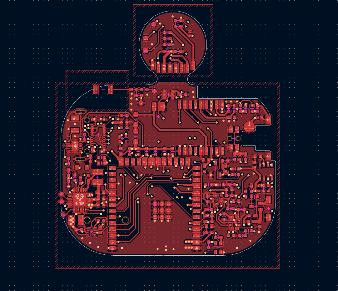
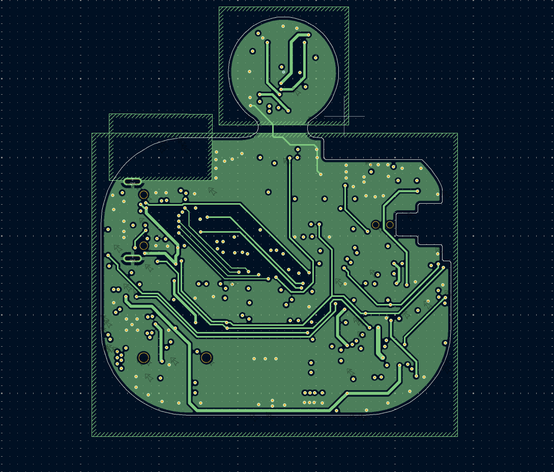
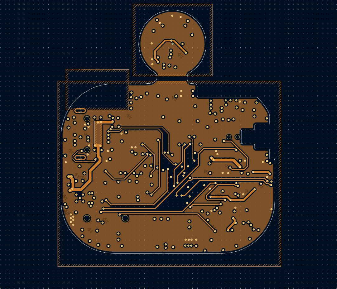
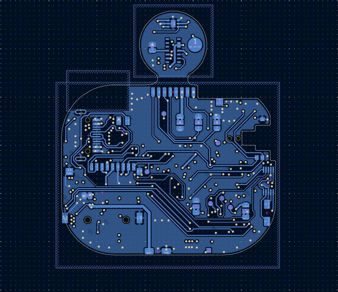
The design is two 1 mm 4-layer PCBs — a main top board carrying nearly everything, and a small skin-facing daughter board for the optical and temperature sensors. They are drawn and fabricated as a single panel and cut apart before reflow (see PCB below).
Schematic capture is complete. Because the part count is high, the schematic is split into one root sheet plus six subsheets, each a functional block:
- 1 · ESP32-S3 WROOM — MCU, crown encoder, SD, display connector, BLE antenna, TVS
- 2 · Power Management — BQ25619 charger, TPS62840 buck, 1.8 V LDO, USB-C
- 3 · Space & Time Sensors — GPS, IMU/ECG, magnetometer, RTC
- 4 · Air Sensors — BME688, PDM microphone
- 5 · Lights — status RGB, flashlight, ambient-light sensor
- 6 · Skin Sensors & LRA — daughter board (MAX30101, TMP117) + haptic driver
The driving idea was to fit every sensor that physically would fit, then leave a few spare test pads for anyone (the author included) who wants to tinker with alternatives. It isn't a lavish amount of slack — the board is dense — but the breakouts are there.
Schematic & source
Printed schematic (PDF):
Kompic_Mk1-Schematic_iv7.1.pdf
KiCad project (editable source):
hardware/Kompic_Mk1
Circuit — Design Decisions
The brain — ESP32-S3-WROOM-1U
The MCU is the strongest part that fit the form factor: a dual-core Xtensa LX7 at 240 MHz with 8 MB PSRAM and 16 MB flash. That compute surplus is the whole point — it exists to run on-device ML (sleep staging, sound classification, sensor fusion), not just to display numbers. Two of the sensors lean the same way: the LSM6DSV16X IMU has an on-chip ML core (decision trees), and the BME688 ships with a gas-classification feature of its own.
The strapping-pin saga — zero slack on 32 GPIOs
Every usable GPIO is assigned; there is no spare pin. Three of the module's pins (GPIO35–37) are eaten by the octal PSRAM and never come out. What's left had to be allocated around the ESP32's boot-time strapping pins and its limited set of RTC-capable pins, which forced a chain of deliberate choices:
Wake sources must land on RTC GPIOs (≤21). Anything that has to wake the watch from deep sleep — tap-to-wake (touch INT), PPG FIFO (MAX30101 INT), raise-to-wake (IMU INT), the RTC alarm, the button, and the crown turn — is pinned to an RTC-capable line and kept there.
I²C stays off the boot-log pins. GPIO43/44 emit ~3 ms of UART boot chatter at reset; a live I²C bus there would be corrupted. So only boot-tolerant signals live on them (an encoder line and a driven touch-reset), never a bus.
The strap pins keep their default levels. The QSPI display lines that double as VDD_SPI / boot-message straps (TE, the 1PPS pin, the display reset) get no external pull-ups — adding one would corrupt flash-voltage selection or the boot mode. They are driven by firmware and the panel after boot instead.
Full GPIO assignment (iv7.1)
| GPIO | Signal | Notes |
|---|---|---|
| 0 | DRV_EN | strap (boot-mode); driven as FW output |
| 1 / 2 | SDA / SCL (bus 1) | 5.1k → 3V3 |
| 3 | QSPI RESET (display) | strap; no pull, panel + FW driven |
| 4 / 5 | SDA / SCL (bus 2) | 5.1k → 3V3 |
| 6 | TP-INT | wake: tap |
| 7 | MAX_INT | wake: PPG FIFO |
| 8 | LSM_INT1 | wake: raise-to-wake |
| 9–14 | QSPI D2/CS/D0/CLK/D1/D3 | display, SPI2/FSPI IOMUX (CS = 10) |
| 15 | RTC_INT | wake: alarm |
| 16 | BQ_BUTTON | wake: button + ship-mode exit; dual-wired to BQ QON |
| 17 / 18 | GPS TX / RX | UART1 IOMUX |
| 19 / 20 | USB D- / D+ | fixed (native USB) |
| 21 | EC_SigA (crown) | wake: crown turn (bonus) |
| 35–37 | PSRAM | unavailable |
| 38–40 | SD CLK / CMD / DAT0 | 1-bit SD |
| 41 | Flashlight gate | ext pull-down |
| 42 | WS2812 data | signal RGB LED |
| 43 | EC_SigB (crown) | boot-log TX — FW ignores pre-init edge |
| 44 | TP-RST | boot-log RX — driven reset, blip harmless |
| 45 | QSPI_TE | strap (VDD_SPI); NO external pull-up |
| 46 | TimePulse (1PPS) | strap (boot-msg); no pull |
| 47 / 48 | Mic CLK / Dout | PDM |
BLE radio
The WROOM-1U routes RF out to a Johanson 2450AT18A100E chip antenna in the top-left corner, through a small matching network (1 pF series, 2.7 nH shunt, 3.9 nH series). That network is an (un)educated guess: a proper LC match needs the physical board sent off for measurement, which realistically won't happen, so the values are a best-effort shot in the dark — it may end up needing a different network, or none. See Known limitations for the antenna-area and U.FL pigtail caveats that go with this.
Power architecture
USB-C 5 V feeds the BQ25619 switching charger, which produces the SYS rail from the LiPo. SYS feeds a TPS62840 buck for the main logic rail, which in turn feeds an XC6206 LDO for 1.8 V. A firmware-gated 5 V boost off the BQ PMID powers the LED loads and the MAX30101's LED driver.
- The logic rail is 3.2 V, not 3.3 V. Two reasons: a small safety margin for every part on it, and the VSET resistor for 3.2 V (100 k) is a stocked Basic part, where 3.3 V would need a 267 k that isn't. Every 3.3 V part runs happily at 3.2 V.
- Two backup power sources, both diode-isolated so they can't discharge back into the rail. A 0.22 F supercap holds the GPS for a ~2 hr hot-start window (a real power saving on re-acquire), and an ML621 rechargeable cell keeps the RTC running. Both are ~3.0 V rated and fine on the 3.2 V charge.
- The crown's tactile button does double duty. Pin budget was tight, so the button is both a general-purpose input and the wake line that pulls the BQ25619 out of shipping mode (dual-wired to the charger's QON).
- An NTC thermistor watches the battery. A 10 k NTC in the BQ's TS divider gates charging by temperature — basic diligence for a LiPo in a sealed case.
How long does the RTC backup actually last?
The PCF85063A's timekeeping draw — CLKOUT disabled (JP5 = GND), I²C idle — is about 220 nA typical at 25 °C (datasheet Rev. 7.2). On the ML621's ~5.5 mAh:
5.5 mAh ÷ 0.22 µA ≈ 25,000 h ≈ ~2.9 years (ideal, typ)
Worst case (datasheet max 450 nA at 25 °C) is ~1.4 years; a warmer wrist-side ~30–40 °C pushes the typical toward 250 nA (~2.5 years). Self-discharge and the charge-limit diode's leakage take more off the top, so realistically call it a couple of years on a full charge — not the "~4 years" quoted in older notes. And in normal use the cell is being topped up from the rail the whole time the watch is powered; this figure is the no-main-power hold time.
Space & time sensors
- GPS (u-blox M10S) sits on I²C bus 1, with solder jumpers to switch it to UART (UART is the default) and to enable SAFEBOOT. VCC_RF is supported but off by default, since the current ceramic antenna is passive.
- Precise time is a headline feature, so the GPS 1PPS gets its own pin. The M10S emits a TimePulse (1PPS) signal into a dedicated ESP32 GPIO; firmware uses that edge to discipline and sync the PCF85063 RTC. The RTC then holds accurate time between fixes. (TimePulse is the GPS's output — the RTC is what it corrects, not its source.)
- Magnetometer (LIS3MDL) has a solder jumper to switch between I²C and SPI. This one is possibly vestigial — everything is already wired for I²C and it's unclear which pins SPI would even use, so it may be removed in a later rev.
- The IMU carries the ECG. The LSM6DSV16X's Qvar inputs form a single-lead ECG; the Qvar2 electrode lives here and connects up to the crown through a pogo pin.
Air sensors
- BME688 — classic I²C connection; the "AI-powered" gas/air-quality sensor.
- MEMS microphone (MSM261DGT003) — a digital PDM part, so there's no analog front-end or ADC step to design around. CLK out, data in.
Lights
- WS2812B status RGB — addressable, so it needs a single dedicated data pin (no I²C), which is fine.
- Flashlight LED — its gate is voltage-driven rather than just switched, giving variable brightness.
Skin sensors & haptics
- MAX30101 + TMP117 on the daughter board — classic I²C. The daughter also carries the Qvar1 electrode, the one that contacts the wrist.
- The DRV2605 haptic driver is on the MAIN board underside, not the daughter — worth stating plainly because the schematic groups it with the skin-sensor sheet. It sits close to the LRA motor's wire pads.
- DRV enable solder jumper (JP12). Default routes EN to a GPIO so firmware can cut the driver overnight for power; tie it high instead and you free that GPIO back up.
Two I²C buses
Two buses, split to dodge an address collision (the DRV2605 and CST9217 touch both want 0x5A). The slow, inert devices — DRV2605 and the BQ25619 — sit on bus 2; everything else lives on bus 1.
| Bus 1 (GPIO1/2) | Bus 2 (GPIO4/5) |
|---|---|
| VEML6030 (0x10), LIS3MDL (0x1C), MAX-M10S (0x42), TMP117 (0x48), PCF85063 (0x51), MAX30101 (0x57), CST9217 (0x5A), LSM6DSV16X (0x6B), BME688 (0x76) | DRV2605 (0x5A), BQ25619 (0x6A) |
PCB — Design Decisions
Panelization & stackup
The main and daughter boards are drawn and fabricated together as one panel, then sawed and filed apart before reflow. It's purely a cost call — this build is involved enough already, and ten minutes with a saw saves real money on a small run.
The stackup is 1 mm, 4-layer: the thinnest 4-layer the fabricator offers cheaply (0.8 mm costs more), and four layers are what the density needs.
| Layer | Role |
|---|---|
| L1 — Top | Components + signals + GND fill; QSPI and the BQ25619 switching loop |
| L2 — Inner 1 | Solid ground plane, unbroken under the high-speed traces |
| L3 — Inner 2 | 3.3 V plane + SYS / 1.8 V / 5 V power |
| L4 — Bottom | Signals + GND fill; I²C, UART, interrupts, underside parts |
Trace widths
| Width | Use |
|---|---|
| 0.17 mm | RF / 50 Ω controlled (BLE, GPS) — not yet recalculated for the 1 mm stackup |
| 0.2 mm | General signals — QSPI, USB, I²C, UART, PDM, interrupts |
| 0.4 mm | Power rails |
| up to 0.6 mm | High current — charger switch node, battery, VBUS |
Placement philosophy
Placement was driven by two things: the physical constraints of the parts (which face which way, what stacks under what) and their usefulness in the worn position. It took a lot of reshuffling and it's good now — not perfect, but Mk II can improve it, especially once the WROOM module is broken into discrete parts and the height it claims is recovered.
Orientation note: positions below are described as if you're reading the watch on your wrist — the crown is on the right edge.
Main board — top side
- Crown side (right edge): the tactile button, the Qvar2 pogo pin, the encoder, and the crown interface.
- Top edge (facing away from you): the VEML6030 ambient-light sensor (aimed outward) and the eight solder pads for the daughter-board wires.
- Top-right corner: the GPS module and its ceramic antenna, aimed outward; the GPS supercap tucked just inboard of it, beneath the VEML.
- Lower-right: the 1.8 V LDO, the BME688, and the MEMS mic.
- Bottom-right: the magnetometer and the flashlight LED.
- Bottom (toward you): the IMU and the signal RGB LED facing the user.
- Bottom-center: the WROOM module, which claims a big chunk of the board.
- Lower-left: the 3.2 V buck.
- Left edge: the BQ25619 charger.
- Left-center: the RTC and the display connector.
- Upper-left corner: the BLE antenna keep-out zone.
The NTC sits on the top side, positioned over where the battery's center lands; the battery itself is mounted on the underside, so the thermistor reads it through the board with thermal vias between them.
Main board — underside
- DRV2605 under the BME/mic region.
- USB-C jack under the RTC and display connector.
- SD card socket toward the bottom-left, with the LRA motor sitting ~0.5 mm beneath it (the motor lives in its own case pocket, two wires to nearby pads).
- Battery pads under the ESP, as close to it as they'd go.
- The 380 mAh LiPo occupies most of one side, sitting under the GPS, 1.8 V reg, magnetometer, IMU, and most of the ESP.
- Three test pads beside the BQ: PMID_GOOD, BQ_STAT, BQ_INT.
Daughter board
- Top: the caps and resistors, the Qvar1 electrode, the eight solder pads, and SDA/SCL tap pads if you want to probe the bus.
- Underside: the MAX30101, the TMP117, and the Qvar1 pogo contact pad.
The two boards join with an eight-conductor link (J2 ↔ J3): I²C bus 1, MAX_INT, the Qvar1 electrode line, the +5 V / +3.3 V / +1.8 V rails, and ground.
Layout care
- Heavy via stitching around the BLE and GPS antenna lines.
- The ESP32's 3.3 V and ground each get four vias down to their planes.
- The BQ switching node is parked in the bottom-left corner, as far as possible from the delicate sensors — to be verified on the prototype.
Known Limitations & Mk II
Honest list of what's shaky on these boards and what the next revision should fix.
RF is the weak spot
The 50 Ω RF traces (BLE, GPS) are 0.17 mm and were not recalculated for the 1 mm stackup. That width carried over from the earlier 0.8 mm design; the correct 50 Ω width for the actual 1 mm 4-layer build is almost certainly different, so antenna performance on these boards is suspect until it's re-derived.
The BLE match network is a guess — a proper LC match needs the physical board measured, which realistically won't happen, so the network may need different values or none at all. At a minimum the antenna wants more board area than it got.
The U.FL pigtail is a hand-soldered kludge. The WROOM-1U brings RF out on a U.FL connector; the antenna's matching pigtail plugs into it, then gets cut to length and its signal and ground soldered back to PCB pads next to the antenna area. It works, but it's fiddly and not how this should be done.
- GPS antenna routing drops through a via before reaching the antenna — not ideal for RF. Mk II fix.
- Compass SPI/I²C jumper is likely vestigial and a candidate for removal.
- Daughter-board wires → flex. The eight-wire bundle and its solder pads should become a flex daughter board that plugs into a standard FPC connector on the main board.
- Proper connectors for the battery, crown, and LRA instead of flying leads to pads.
- Decompose the WROOM module into discrete ESP32-S3 + flash/PSRAM + RF front-end. That reclaims significant board area and lets the RF section move somewhere antenna-friendly — the highest-leverage change for Mk II, and the one that would clear up most of the RF problems above.