Starting off right
This guide walks you through the complete manufacturing process for the Nosey MEMS Mk2, from ordering PCBs to final assembly and testing. Remember that a full nasometer needs two Mk2 boards — one for the nasal channel and one for the oral channel — so order in pairs.
Currently, the full PCB manufacturing and assembly has only been tried via JLCPCB. All present information is for their specific ordering steps. If you are using a different manufacturer (or even this one at a later date), please adjust accordingly!
All the files required for manufacture will be available at the GitHub repo after quality control.
Nosey MEMS Mk2 is designed to be manufactured as simply, as easily, and as cheaply as possible.
- The PCB is small (25 × 50 mm), keeping both the PCB manufacturing cost and the final device footprint low.
- Assembly is only done on the Top layer, simplifying the process.
- All top-side components, excluding the XLR3 jack and the four bottom-side electrolytic capacitors, are assembled for us, minimizing post-assembly work.
- Automatic assembly allows us to pick smaller part packages, lowering the parts cost and allowing for a smaller footprint, albeit with a possible increase in difficulty for manual rework.
- The use of a MEMS microphone circumvents a lot of obstacles in microphone design and manufacture — from sourcing parts to soldering — while keeping the cost low at an acceptable frequency range.
- A fully built Mk2 board comes out to roughly €20, and a batch of 10 boards with assembly (excluding the manually fitted parts) is about €65.
The Process of Acquiring a Nosey MEMS Mk2
Step by step.
Getting the Production Files
Go to Downloads and download the production folder. Inside there are:
- the .zip file containing the PCB Gerber files,
- the bom.csv file containing the Bill of Materials, and
- the positions.csv file containing the component placements (CPL).
Find a PCB fabrication and component assembly manufacturer and follow the general ordering process. The rest of the guide references the process of a particular manufacturer.
PCB Fabrication
Upload the .zip Gerber files. Choose fabrication options to your liking. The settings used for the verified Mk2 run are in Table 1.
| Spec | Value |
|---|---|
| Dimensions (if using the source PCB) | 25 mm × 50 mm |
| Material Type | FR4 TG135 |
| PCB Thickness | 1.6 mm |
| Layers | 2 |
| Surface Finish | Lead-free HASL |
| Outer Copper Weight | 1 oz |
| Via Covering | Tented |
| PCB Color | Blue |
| Silkscreen | White |
| Deburring / Edge Rounding | Yes |
| Board Outline Tolerance | ±0.2 mm |
| Confirm Production File | Yes |
The only options changed from the manufacturer's defaults were: blue solder mask, lead-free HASL surface finish, confirm production file, and deburred / edge-rounded edges. Everything else was left at the standard 2-layer, 1.6 mm defaults.
Bill of Materials
The top-side, machine-assembled components are listed in Table 2. This is a 13-line BOM (13 distinct parts), all confirmed for the verified run.
| Component | Designator | Footprint | JLCPCB Part # |
|---|---|---|---|
| 47R | R6, R7 | 0805 | C17714 |
| 470R | R10 | 0805 | C17710 |
| 3k | R2, R3 | 0805 | C17661 |
| 15k | R1, R4, R5, R8, R9 | 0805 | C17475 |
| 10nF | C10 | 0805 | C1710 |
| 22nF | C5, C6 | 0805 | C1729 |
| 2.2uF | C1, C4, C9 | 0805 | C377773 |
| 10uF | C11, C12, C13 | 0805 | C440198 |
| 1N4148 | D1, D3 | D_SOD-323 | C2128 |
| 1SMA4746A (18V Zener) | D2 | D_SMA | C22387572 |
| OPA1652 | U1 | SOIC-8_3.9x4.9mm_P1.27mm | C30025 |
| PJ71K30SC | U2 | SOT-23 | C411738 |
| NA-FFA381-A10-1 | MK1 | 2.75×1.85×1.0mm Top Port | C50275774 |
These are the chosen components available at the time. Where possible, select the Basic parts the manufacturer offers automatically; the OPA1652 (U1) is an Extended part and may need to be located separately.
Part numbers drift over time and between suppliers. Please adjust according to your need and your manufacturer.
Bottom-side / manually fitted parts
The components in Table 3 are not machine-assembled. They are sourced separately and hand-soldered after the boards arrive (see Soldering).
| Component | Designator | Notes |
|---|---|---|
| 47uF 63V electrolytic | C2, C3, C7, C8 | Four through-hole electrolytic caps on the bottom side |
| XLR3 jack | J1 | Combined phantom power input and balanced audio output |
Assembly Instructions
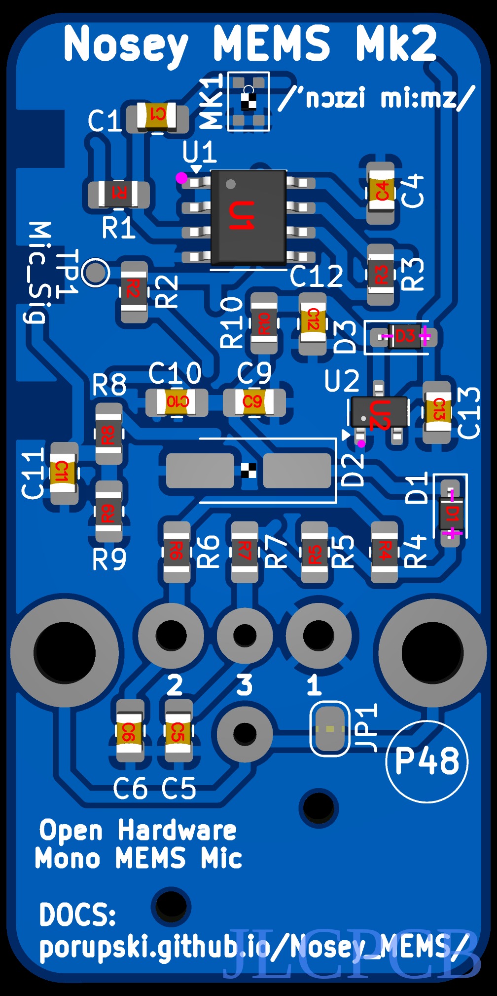
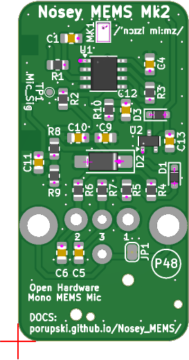
After confirming the BOM file, the component placements (CPL) need to be verified next. Sometimes the orientation of components may be wrong. Carefully inspect and make sure all polarities are correct. The assembly placement for the verified run is shown in Figure 1.
NOTE:
When uploading the BOM and CPL, the assembler may flag the following: "TP1, H1, H2, JP1 designators don't exist in the BOM file." This is expected — TP1 is a test pad, H1/H2 are baffle mounting holes, and JP1 is the shield-to-ground jumper. None of them are placed parts, so you can simply continue.
If the manufacturer's viewer doesn't show the model for the MEMS microphone (MK1), the manufacturer should resolve this. Otherwise, a soldering station and advanced SMD soldering skills will be needed to solder the MEMS microphone manually on.
If a component is placed in the wrong orientation, the manufacturer typically runs a Design for Manufacturability (DFM) analysis to catch such mistakes. While this provides a useful safety net, it's best practice to ensure all components are oriented correctly before submitting the design.
For the verified run, the PCBA was ordered with the following parameters:
- PCBA Type: Economic
- Assembly Side: Top side
- PCBA Qty: 10
- Tooling holes: Added by the manufacturer
- Confirm Parts Placement: Yes
- Solder Paste: High temp
- Reflow: Nitrogen reflow soldering (standard for Economic)
- Packaging: Antistatic bubble film

Soldering
Upon receiving the boards, the components that still require hand-soldering are the four bottom-side 47 µF 63 V electrolytic capacitors (C2, C3, C7, C8) and the XLR3 audio jack (J1).
- Fit the four electrolytic capacitors in their bottom-side positions (C2, C3, C7, C8), observing polarity carefully
- Place the XLR3 jack in its designated position on the PCB (J1)
- Solder all pins with appropriate solder and flux
- Verify all connections are mechanically and electrically sound
- Proceed to Testing and Verification


This concludes the soldering process. If all went well, the Nosey MEMS Mk2 is now ready for testing. For optional modifications, see Modifications below. Otherwise, proceed to Testing.
Modifications
The following modifications are optional and may be added in future revisions of this guide.
Jackless Nosey MEMS Mk2
If sourcing an XLR3 jack is difficult or not necessary for the application, audio cables can be soldered directly to the PCB pads. Additional strain relief should be added (e.g., zip-ties to the 3D-printed mount) to prevent damage to solder joints from cable movement.
Figure and 3D-printed cable adapter design to be added.
Shield to Ground Connection
Connecting the cable shield to ground is a debated topic in audio applications. On Mk2 this is selectable by jumping JP1. This modification will be tested and documented in a future update with measured results showing any impact on noise floor and interference rejection.
Measurement results and implementation guide to be added.
5V Operation
For advanced users only. By default the Mk2 runs the OPA1652 from the 18V Zener-clamped rail and supplies the MEMS via the PJ71K30SC (3.3V) LDO. To run on a 5V rail instead, fit the 5V LDO variant (PJ71K50SC), cut the traces between pads 1–2 on both JP2 and JP3, and solder across pads 2–3. This routes a 5V supply to the op-amp and a 2.5V (V/2) bias to the MEMS. Only recommended for users experienced with analog audio circuit design. Details can be found in the schematics file.
Read the modification notes on the schematic carefully before attempting.
Testing & Verification
How to test your completed board to ensure proper functionality. Repeat the whole process for each of the two boards.
- First, visually inspect the board. Is it neat? Is it clean? Are all the parts neatly placed and soldered? Are any crooked? Are all components making electrical contact? Does any component look damaged? Are all the polarized components (diodes, electrolytic capacitors, op-amp) correctly oriented?
- Second, turn off Phantom power (48V) and, provided the board is up to standard, connect the Nosey MEMS Mk2 to an audio capture card with a shielded balanced XLR cable. Verify there are no sounds coming from the board, as it is not yet powered.
- Third, set the gain to zero before turning on Phantom power (48V).
- Fourth, slowly increase the gain, making sure there is no feedback or irregular sounds, and try talking into the MEMS microphone. You should hear yourself clearly, with no distortion, delay or artefacts.
- Fifth, repeat the process for the second board and verify that both work correctly and equally well — matched behaviour between the two boards is what makes the nasalance ratio meaningful.
- Sixth, congratulations on your working pair of Nosey MEMS Mk2 boards!
If the verification process was successful, move on to calibration of the devices, or to 3D Printing the parts. If the verification failed, try Troubleshooting.
Troubleshooting
Common issues and how to resolve them.
PCB Visual Inspection
- Check overall board cleanliness and neatness of component placement
- Verify all components are properly seated, straight, and free from physical damage
- Confirm correct orientation of all polarized components (diodes, electrolytic capacitors, the op-amp)
- Look for any bent pins, damaged traces, or signs of thermal stress
PCB Electrical Inspection
- Verify phantom power is enabled and measures 48V at the XLR connector
- Measure the regulated supply rail — it should read approximately 18V (Zener-clamped) at the supply test pads (T_Vcc1 / T_Vcc2)
- Measure the V/2 virtual ground — it should read about half of the supply, approximately 9V (T_V/2)
- Confirm the MEMS supply rail is at 3.3V (PJ71K30SC LDO output)
- Check for an output signal from the op-amp at the audio test pad (T_Sig), referenced to ground (T_Gnd)
- Inspect all solder joints for proper flow and electrical contact — look for cold joints or bridged connections
- Examine PCB traces for damage, lifted pads, or unintended continuity between nets
- Use a multimeter in continuity mode to check for shorts between power rails and ground
Audio Chain Verification
- Confirm the audio interface is powered on, connected to the computer, and recognized by the system
- Test XLR cables and connectors with a known-good microphone to rule out cable faults
- Verify the Nosey MEMS Mk2 is properly seated and making good electrical contact
- Set audio interface gain to minimum (0 dB) and ensure the channel is unmuted
- Confirm correct input/output routing in your DAW or REW software
- Check that phantom power is reaching the microphone through the entire signal chain